- 您现在的位置:买卖IC网 > Sheet目录332 > IR21834STRPBF (International Rectifier)IC DRIVER HALF BRIDGE 14SOIC
�� �
�
�Data� Sheet� No.� PD60173� rev.H�
�IR2183� (� 4� )(S)� &� (PbF)�
�Features�
�?� Floating� channel� designed� for� bootstrap� operation�
�Fully� operational� to� +600V�
�Tolerant� to� negative� transient� voltage�
�HALF-BRIDGE� DRIVER�
�Packages�
�14-Lead� PDIP�
�?�
�?�
�?�
�?�
�?�
�?�
�?�
�?�
�dV/dt� immune�
�Gate� drive� supply� range� from� 10� to� 20V�
�Undervoltage� lockout� for� both� channels�
�3.3V� and� 5V� input� logic� compatible�
�Matched� propagation� delay� for� both� channels�
�Logic� and� power� ground� +/-� 5V� offset.�
�Lower� di/dt� gate� driver� for� better� noise� immunity�
�Output� source/sink� current� capability� 1.4A/1.8A�
�Also� available� LEAD-FREE� (PbF)�
�8-Lead� PDIP�
�IR2183�
�8-Lead� SOIC�
�IR2183S�
�IR21834�
�14-Lead� SOIC�
�IR21834S�
�Description�
�The� IR2183(4)(S)� are� high� voltage,�
�high� speed� power� MOSFET� and� IGBT�
�drivers� with� dependent� high� and� low�
�side� referenced� output� channels.� Pro-�
�prietary� HVIC� and� latch� immune�
�IR2181/IR2183/IR2184� Feature� Comparison�
�Cross-�
�Input� conduction�
�Part� Dead-Time� Ground� Pins� Ton/Toff�
�logic� prevention�
�logic�
�2181� COM�
�HIN/LIN� no� none� 180/220� ns�
�21814� VSS/COM�
�CMOS� technologies� enable� rugge-�
�dized� monolithic� construction.� The�
�logic� input� is� compatible� with� standard�
�2183� Internal� 500ns� COM�
�HIN/LIN� yes�
�21834� Program� 0.4� ~� 5� us� VSS/COM�
�2184� Internal� 500ns� COM�
�IN/SD� yes�
�21844� Program� 0.4� ~� 5� us� VSS/COM�
�180/220� ns�
�680/270� ns�
�CMOS� or� LSTTL� output,� down� to� 3.3V�
�logic.� The� output� drivers� feature� a� high� pulse� current� buffer� stage� designed� for� minimum� driver� cross-conduction.�
�The� floating� channel� can� be� used� to� drive� an� N-channel� power� MOSFET� or� IGBT� in� the� high� side� configuration�
�which� operates� up� to� 600� volts.�
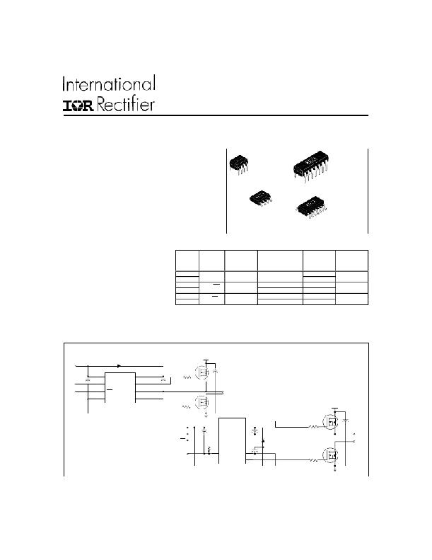
�Typical� Connection�
�up� to� 600V�
�V� CC�
�V� CC�
�V� B�
�HIN�
�HIN�
�HO�
�LIN�
�LIN�
�COM�
�V� S�
�LO�
�TO�
�LOAD�
�IR2183�
�HO�
�IR21834�
�up� to� 600V�
�V� CC�
�V� CC�
�V� B�
�(Refer� to� Lead� Assignment� for� correct� pin�
�HIN�
�LIN�
�HIN�
�LIN�
�DT�
�V� S�
�TO�
�LOAD�
�configuration)� This/These� diagram(s)� show�
�electrical� connections� only.� Please� refer� to� our�
�V� SS�
�R� DT�
�V� SS�
�COM�
�LO�
�Application� Notes� and� DesignTips� for� proper� circuit�
�board� layout.�
�www.irf.com�
�1�
�发布紧急采购,3分钟左右您将得到回复。
相关PDF资料
IR21844SPBF
IC DRIVER HIGH/LOW SIDE 14SOIC
IR2213SPBF
IC DRIVER HIGH/LOW SIDE 16SOIC
IR22141SSPBF
IC DRIVER HALF BRIDGE SGL 24SSOP
IR2235JPBF
IC DRIVER BRIDGE 3PHASE 44PLCC
IR2301PBF
IC DRIVER HIGH/LOW SIDE 8DIP
IR2302PBF
IC DRIVER HALF BRIDGE 8DIP
IR2304SPBF
IC DRIVER HALF BRIDGE 8-SOIC
IR2308SPBF
IC DRIVER HALF BRIDGE HV 8SOIC
相关代理商/技术参数
IR2183PBF
功能描述:功率驱动器IC Hlf Brdg Drvr Soft Trn On 500ns RoHS:否 制造商:Micrel 产品:MOSFET Gate Drivers 类型:Low Cost High or Low Side MOSFET Driver 上升时间: 下降时间: 电源电压-最大:30 V 电源电压-最小:2.75 V 电源电流: 最大功率耗散: 最大工作温度:+ 85 C 安装风格:SMD/SMT 封装 / 箱体:SOIC-8 封装:Tube
IR2183S
功能描述:IC DRIVER HALFBRIDGE 600V 8-SOIC RoHS:否 类别:集成电路 (IC) >> PMIC - MOSFET,电桥驱动器 - 外部开关 系列:- 标准包装:50 系列:- 配置:高端 输入类型:非反相 延迟时间:200ns 电流 - 峰:250mA 配置数:1 输出数:1 高端电压 - 最大(自引导启动):600V 电源电压:12 V ~ 20 V 工作温度:-40°C ~ 125°C 安装类型:通孔 封装/外壳:8-DIP(0.300",7.62mm) 供应商设备封装:8-DIP 包装:管件 其它名称:*IR2127
IR2183SPBF
功能描述:功率驱动器IC HALF BRDG DRVR 600V 10 to 20V 1.4A RoHS:否 制造商:Micrel 产品:MOSFET Gate Drivers 类型:Low Cost High or Low Side MOSFET Driver 上升时间: 下降时间: 电源电压-最大:30 V 电源电压-最小:2.75 V 电源电流: 最大功率耗散: 最大工作温度:+ 85 C 安装风格:SMD/SMT 封装 / 箱体:SOIC-8 封装:Tube
IR2183STR
功能描述:IC DRIVER HALFBRIDGE 600V 8-SOIC RoHS:否 类别:集成电路 (IC) >> PMIC - MOSFET,电桥驱动器 - 外部开关 系列:- 标准包装:50 系列:- 配置:高端 输入类型:非反相 延迟时间:200ns 电流 - 峰:250mA 配置数:1 输出数:1 高端电压 - 最大(自引导启动):600V 电源电压:12 V ~ 20 V 工作温度:-40°C ~ 125°C 安装类型:通孔 封装/外壳:8-DIP(0.300",7.62mm) 供应商设备封装:8-DIP 包装:管件 其它名称:*IR2127
IR2183STRPBF
功能描述:功率驱动器IC Hlf Brdg Drvr Soft Trn On 500ns RoHS:否 制造商:Micrel 产品:MOSFET Gate Drivers 类型:Low Cost High or Low Side MOSFET Driver 上升时间: 下降时间: 电源电压-最大:30 V 电源电压-最小:2.75 V 电源电流: 最大功率耗散: 最大工作温度:+ 85 C 安装风格:SMD/SMT 封装 / 箱体:SOIC-8 封装:Tube
IR2184
功能描述:IC DRIVER HIGH/LOW SIDE 8-DIP RoHS:否 类别:集成电路 (IC) >> PMIC - MOSFET,电桥驱动器 - 外部开关 系列:- 标准包装:50 系列:- 配置:低端 输入类型:非反相 延迟时间:40ns 电流 - 峰:9A 配置数:1 输出数:1 高端电压 - 最大(自引导启动):- 电源电压:4.5 V ~ 35 V 工作温度:-40°C ~ 125°C 安装类型:表面贴装 封装/外壳:TO-263-6,D²Pak(5 引线+接片),TO-263BA 供应商设备封装:TO-263 包装:管件
IR21844
功能描述:IC DRIVER HIGH/LOW SIDE 14-DIP RoHS:否 类别:集成电路 (IC) >> PMIC - MOSFET,电桥驱动器 - 外部开关 系列:- 标准包装:50 系列:- 配置:低端 输入类型:非反相 延迟时间:40ns 电流 - 峰:9A 配置数:1 输出数:1 高端电压 - 最大(自引导启动):- 电源电压:4.5 V ~ 35 V 工作温度:-40°C ~ 125°C 安装类型:表面贴装 封装/外壳:TO-263-6,D²Pak(5 引线+接片),TO-263BA 供应商设备封装:TO-263 包装:管件
IR21844PBF
功能描述:功率驱动器IC HALF BRDG DRVR 600V 10 to 20V 1.4A
RoHS:否 制造商:Micrel 产品:MOSFET Gate Drivers 类型:Low Cost High or Low Side MOSFET Driver 上升时间: 下降时间: 电源电压-最大:30 V 电源电压-最小:2.75 V 电源电流: 最大功率耗散: 最大工作温度:+ 85 C 安装风格:SMD/SMT 封装 / 箱体:SOIC-8 封装:Tube